Raspberry Pi Pico Ham Radio Transmitter
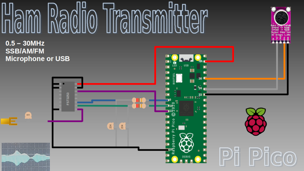
Discover the world of amateur radio with the Raspberry Pi Pico-based Ham Radio Transmitter project, which opens up a spectrum of possibilities for radio enthusiasts. Capable of outputting SSB, AM, and FM signals, this versatile transmitter allows you to cover frequencies from 0.5 to 30MHz, including the Ham bands from 160m to 10m. The transmitter is based on a Raspberry Pi Pico, which uses a powerful PIO feature to output an RF oscillator with precisely controlled phase and frequency, reducing the part count and keeping the cost down. The transmitter also employs a PWM output to generate an RF envelope for amplitude modulation. C++ Code for Pi Pico
Note:
Feel free to experiment, but please keep in mind that it is still an experimental prototype and not a fully tested design. There are areas that still need work and there are likely to be changes as the design evolves.
Prototype Design

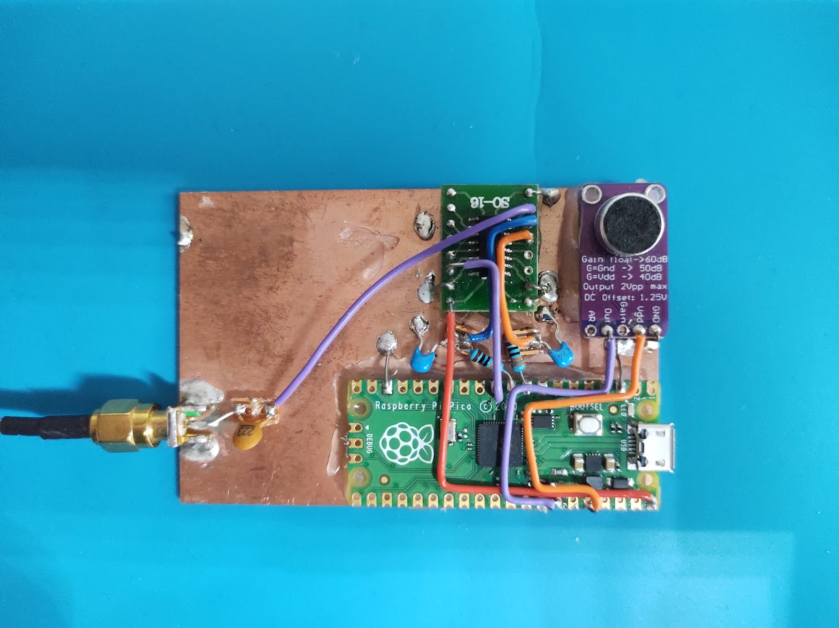
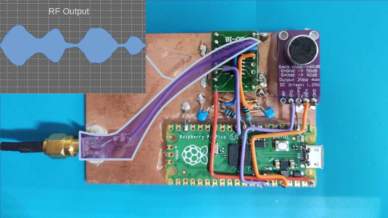
At the moment this is a proof of concept rather than a finished product. I don’t have an amplifier or any filtering yet so it can’t be used on the air. I built a simple prototype on a piece of copper-clad PCB, to test the concept and assess the quality of the output.
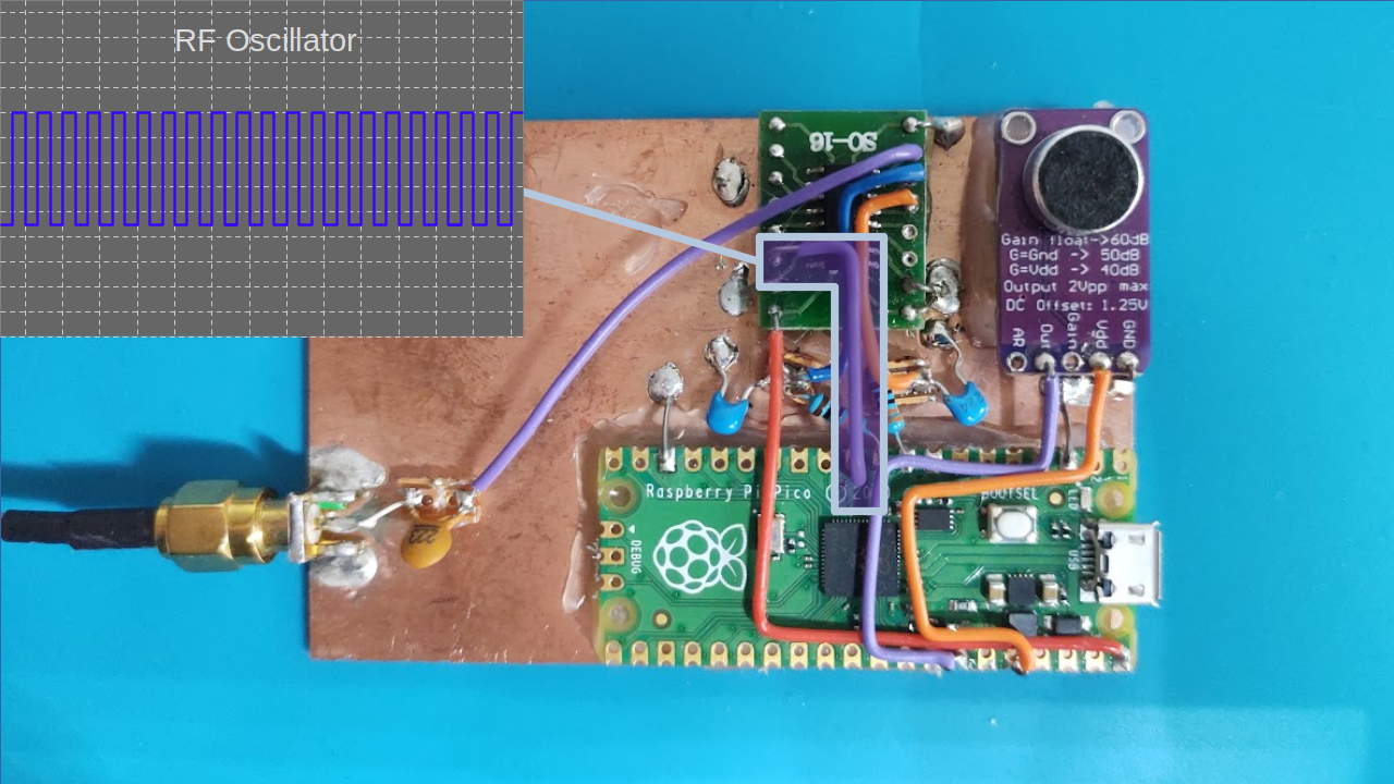
The hardware is pretty simple, the Pi Pico has 3 outputs. The RF oscillator is output on an IO pin, the phase and the frequency are precisely controlled by software.
For constant amplitude modes like CW and FM, this is all we need, but for modes that modulate the amplitude like AM and SSB, we use a complimentary pair of PWM outputs to generate an RF envelope. The PWM outputs are passed through a simple RC low-pass filter with a cut-off frequency of around 3kHz. I run the PWM as fast as I can, to reduce ripple, we can get 8-bits of resolution at around 500kHz, at this frequency the filter attenuation is very strong.
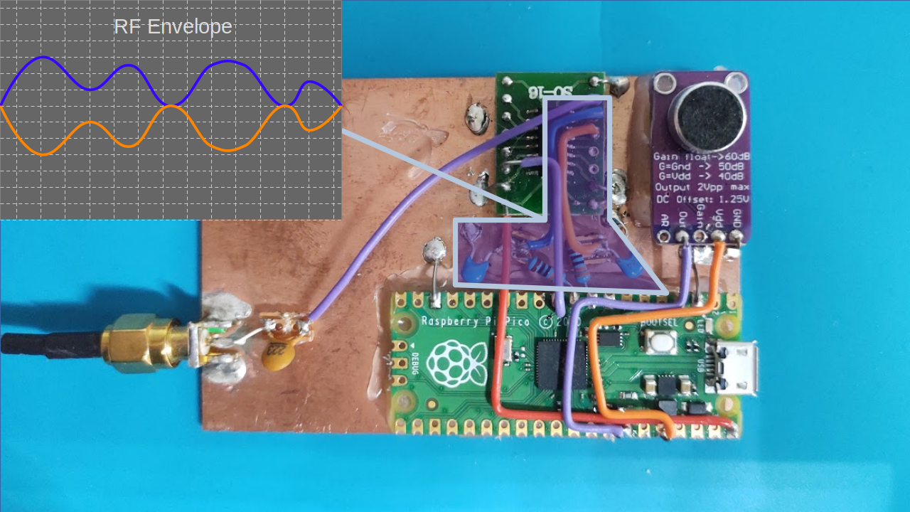
For now, I’m using an FST3253 analogue switch to mix the RF Oscillator and the RF envelope.
I’m using a MAX9814 microphone pre-amplifier model for convenience. The module is self-contained and can be connected straight to the ADC input of the Pi-Pico. The MAX9814 contains an automatic gain control unit, this isn’t really ideal for communication use because it amplifies background noise when you aren’t speaking.
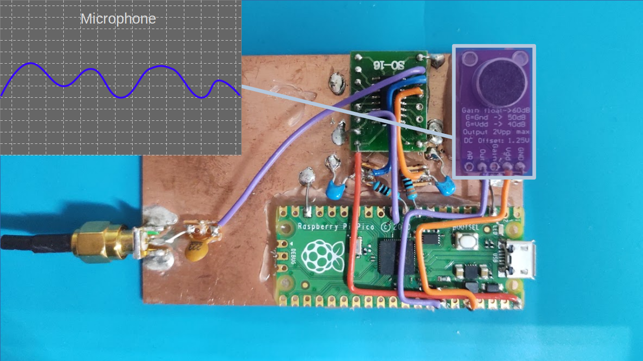
Eventually, I plan to either disable the AGC or use a simple op-amp circuit for the microphone pre-amplifier.
Software Design
RF Oscillator
The software design makes heavy use of the PIO and DMA features of the Pi-Pico and these do most of the heavy lifting. The PIO program is very simple, it uses the auto-pull feature to repeatedly read 32-bit words from the FIFO and output them one bit at a time to an output pin. We have left the divider at the full rate so we output one bit per system clock. At 125MHz, this gives us a theoretical maximum frequency a little over 60MHz.
.program stream_bits
    out pins, 1
In principle the process is simple, a waveform of exactly the right frequency is pre-generated using high-precision arithmetic to reduce long-term frequency errors. The DMA transfers waveforms of a fixed length from memory to the PIO FIFO. The length of the waveform is a compromise between memory consumption and performance. The longer the waveform, the less frequently the DMA needs to be triggered.
Complexity arises because the waveform will not usually contain an exact number of RF cycles. At the end of a 256-bit section of waveform, we will usually be partway through a cycle. To transition smoothly, we need to start part-way through the next waveform. We can choose a starting point that has the correct phase within a clock cycle. We can accumulate any phase error so that we can compensate for it later. Using this technique it is possible to always toggle within a clock cycle of when we should, keeping the jitter to +/- one clock cycle.
The process is further complicated by the transfer size of the PIO. I have chosen to use 32-bit transfers because this minimises the bandwidth consumed by the DMA. Smaller transfers are possible, but the bandwidth would be excessive and it might be difficult to keep up. Instead, I have opted to make 32 copies of the waveform, each advanced by an extra clock cycle. Small advances of less than 32 clocks are made by selecting the appropriate waveform, for longer offsets whole 32-bit words can be added. The software can also advance or retard the waveforms to modulate the phase which we need to generate FM and SSB.
To reduce the computational load on the software, DMA chaining is used to play back batches of 256-bit waveforms without software intervention. A batch of waveforms is started for every audio sample. Batches of 32x256-bit waveforms yield an audio sample rate of about 15kHz for example. Longer and shorter batches can be used at different sample rates.
I have made some measurements and it turns out that the software takes less than 10us to plan and dispatch each batch using less than 10% of the CPU on one core.
Modulator
The modulator converts a signal from the microphone and converts it into a baseband signal feeding the RF section. We need to produce samples in polar (magnitude and phase) rather than rectangular (I and Q) format. The phase component controls the phase of the RF oscillator, while the magnitude controls the PWM to generate the RF envelope.
AM and FM modulation is reasonably simple. In AM modulation, the microphone signal drives the magnitude directly, while the phase is held at zero. FM modulation is only slightly more complicated. In this mode, the phase difference between samples (AKA frequency) is taken from the microphone. In other words, the microphone signal is integrated to generate the phase output. In FM mode, the amplitude is held at the maximum value.
While AM and FM modulation only affects either the phase or magnitude of the signal, SSB modulation requires both the phase and frequency components to be modulated. The SSB signal is first generated in rectangular representation and then converted to phase and magnitude representation using the CORDIC algorithm.
The microphone input consists only of real samples. The I component is taken directly from the microphone input while the Q component is set to zero. Since the imaginary part of the signal is zero, it follows that the frequency spectrum is symmetrical and includes both positive and negative frequency components.

The positive frequency component is the upper sideband, and the negative frequency component is the lower sideband, we need to remove the opposite sideband leaving us with only positive (for USB) or negative (for LSB). One method of achieving this is to use a Hilbert transform, but I find that using frequency shifts and filters is more intuitive, although the process is equivalent.
The process is to up-shift the frequency by Fs/4 using a complex multiplier and filter the signal using a symmetrical half-band filter retaining only the negative frequency components. The frequency is then down-shifted by Fs/4 leaving only the lower sideband.
Fs/4 is chosen because it can be implemented efficiently. A complex sine wave with a frequency of Fs/4 consists of only 0,1 and -1. Multiplication by 0, 1, or -1 can be implemented using trivial arithmetic operations.
Choosing a half-band filter -Fs/4 to Fs/4 allows further efficiency improvements. The kernel of a half-band filter is symmetrical, potentially this can approximately halve the number of multiplication operations, or halve the number of kernel values that need to be stored. In addition to this about half of the kernel values are 0, again approximately halving the number of multiplications. Overall, this filtering operation reduces the number of multiplications needed by an approximate factor of 8.
The structure as shown leaves the lower sideband part of the signal. An upper sideband signal could be generated by first down-shifting the frequency, and then up-shifting. Since the upper and lower sidebands are mirror images, an easier way to switch between upper and lower sidebands is to change the direction of rotation at the output of the modulator by switching the I and Q components for example.
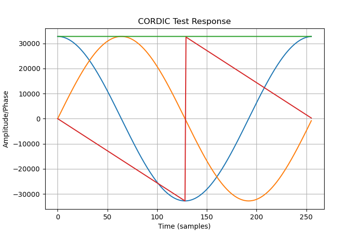
There are quicker approximate methods to calculate the magnitude and phase of a complex signal, I found that these methods resulted in unacceptable spurious signals in the frequency spectrum. Instead, I opted to use the CORDIC algorithm. It isn’t quite as fast as some other methods, but it’s still much faster than library functions like atan2. The nice thing about CORDIC is that we can perform more (or fewer) iterations to achieve the best balance between performance and precision. The CORDIC algorithm turned out to be a good compromise, both fast enough and precise enough for our application.
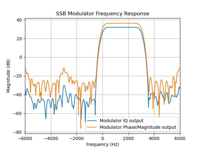
We can characterise the modulator by looking at the impulse response in the frequency domain. We can see that the filter passes half of the positive frequencies while attenuation the negative frequencies. The pass band of 2-3kHz is ideal for SSB transmissions. I have plotted the raw IQ output from the modulator as well as the phase and magnitude output from the CORDIC. The CORDIC causes some degradation to the frequency response, but not excessively.
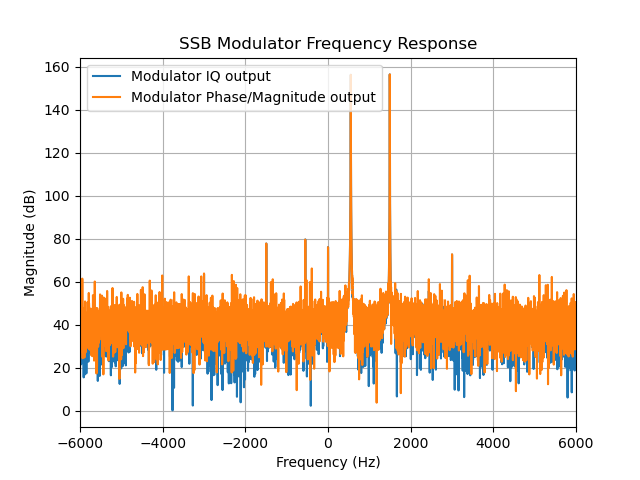
Another useful test is to filter two tones that are not harmonically related. We can see that the negative tones are very strongly attenuated.
Performance
The SSB modulator is the most processor-intensive of the modes. In SSB mode, the modulator adds just over 10% CPU usage to the 10% used by the RF oscillator. In total, we are still using less than 30% of the CPU on a single core, so there is plenty of scope for additional development.
Initial Testing
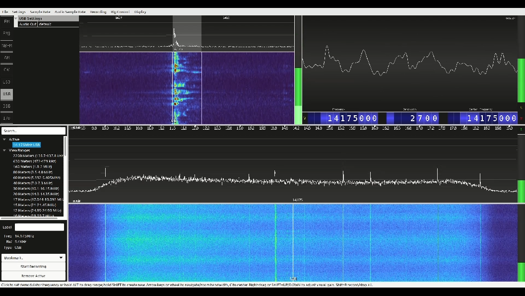
I tested the transmitter in all the modes using an SDR receiver, and the results were very promising with good quality SSB, AM and FM being generated. I also tested with a few different receivers which also gave good results. Check out the Video to see the results.
Amplifier Experiments
So far the transmitter has an output power of around 1 milliwatt. To make this into a practical transmitter, an amplifier is needed. The traditional approach for single-sideband transmissions is to use a linear amplifier that reproduces both the amplitude and phase information in the RF signal. The only real disadvantage of this approach is that linear amplifiers are relatively inefficient because they operate transistors in their linear region.
A class-E RF amplifier is a very efficient class of amplifier that allows efficiencies of greater than 90%. The disadvantages of the class-E amplifier are that it is not linear and removes the amplitude component from the RF signal entirely. It is possible to restore the amplitude information produced by the class-E amplifier by modulating the power supply. This is called polar modulation because the RF signal is reproduced from both the amplitude and phase components. I’m particularly interested in this type of amplifier because of the high efficiency that can potentially be achieved. The high-efficiency design reduces the size and capacity of batteries and removes the need for a large heatsink. This makes a significant contribution to reducing the size, weight, and overall cost.
Class-E RF Amplifier
Class-E amplifiers belong to the category of switching amplifiers. A switching topology is employed to minimize power dissipation by the switching transistor. The amplifier is designed to ensure the transistor switches fully on or fully off. When the transistor is off, it exhibits a very high impedance, resulting in negligible power dissipation. Conversely, when switched fully on, the transistor dissipates minimal power due to its low internal resistance.
Another factor contributing to power loss is the output capacitance. During each cycle, the capacitor undergoes charging and discharging, and the energy stored in the capacitor is released as heat. This becomes especially significant at higher frequencies, even with relatively small capacitance values.
To mitigate these losses, the class-E amplifier strategically combines the parasitic capacitance of the transistor with additional capacitors and inductors to create a resonant circuit. This configuration harnesses the energy stored in the inductors and capacitors, inducing voltage oscillations. Carefully chosen component values ensure that the voltage returns to zero just before the transistor switches on. By preventing energy storage in the capacitor when the transistor is on, the amplifier effectively minimizes energy wastage.
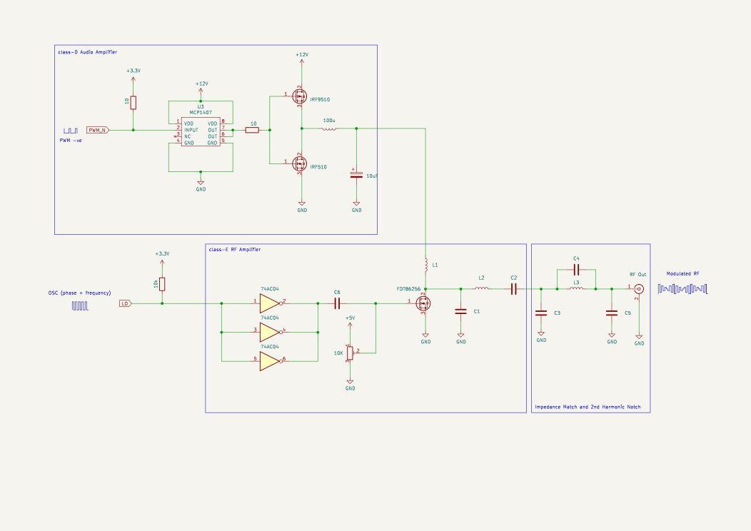
The class-E amplifier itself consists of a single transistor, the gate of the transistor is driven with a saturated version of the RF signal sufficient to switch the transistor on for half of each RF cycle. Power is supplied by an RF choke L1 that allows DC to be supplied to the amplifier while blocking RF frequencies. The inductance of the choke is not critical but it should have an impedance which is much larger than that of the other circuit elements. C1, L2 and C2 form a resonant network. C1 combines with the parasitic capacitance of the transistor to give the required capacitance. The load impedance is calculated to give the required output power at a particular supply voltage. In this design, an impedance of 8 ohms is chosen to give an output power of 5W with a 12V supply. In practice, the impedance of the actual load is not 8 ohms and we need an impedance matching circuit to make the standard 50 ohms load appear to the amplifier as an 8 ohm load. C3, C5 and L3 form a pi impedance matching network to achieve this. The resonant circuits within the class-E amplifier have a band-pass characteristic which attenuates high-order harmonics sufficiently. Adding C4 in parallel with L3 creates an additional notch at the second harmonic frequency further attenuating the second harmonic notch which is prominent in a class-E amplifier.
class-E amplifiers are often regarded as challenging to design, and the associated mathematical calculations can be relatively complex. Despite this, a set of equations can be employed for the amplifier’s design. The commonly used spreadsheet serves this purpose and aids in designing class-E amplifiers.
Although the BS170 and IRF510 have traditionaly been popular choices for home-brew HF amplifiers, the FDT86256 has been used successfully in other designs. The advantages of this device are the very low Coss of only 8pF. The max Vds voltage of 150V and Id of 3A provide plenty of design margin for a 5W amplifier.
To simplify the design process, I developed a Python script based on the equations found in this spreadsheet. The script calculates values for each amateur radio band. It uses standard component values, as opposed to exact ones. Where possible the actual component value is carried forward through the calculations to minimize errors. In practice though, this made little difference to the final results.
Additionally, the script selects an appropriate toroid material and calculates the number of turns required to achieve the desired inductance. It’s essential to note that these calculated values should be considered as a starting point. In real-world scenarios, component errors, parasitic capacitances, and inductances can introduce unpredictable effects. Therefore, some adjustments and tweaking may be necessary to optimize performance and achieve the best results.
load_impedance_ohms = 0.32*psu_voltage*psu_voltage/output_power
load_impedance_ohms -= 1.5*RDSon_ohms
C1_pF = (1e12*0.19)/(2.0*pi*centre_frequency_Hz*load_impedance_ohms)
C1_pF -= Coss_pF
C1_pF = nearest_capacitor(C1_pF)
C2_pF = 1e12/(2.0*pi*centre_frequency_Hz*load_impedance_ohms*1.5)
C2_pF = nearest_capacitor(C2_pF)
L2_uH = (1.8*load_impedance_ohms)+1.0 / (2*pi*centre_frequency_Hz*C2_pF/1e12)
L2_uH = 1e6*L2_uH/(2.0*pi*centre_frequency_Hz)
L2_windings = calculate_inductor_turns(L2_uH)
L1_uH = 15*L2_uH
L1_windings = calculate_inductor_turns(L1_uH)
$python class_e_design.py
Class-E Amplifier Design
========================

Supply Voltage: 12V
Output Power: 5W
RDSon:  0.912ohms
Coss: 8.0pF

       o VDD     Class-E Amplifier        |  Impedance Match and Harmonic Notch
       |                                  |
       |                                  |
     [ L1 ]                               |
       |                                  |        +---[ C4 ]---+
       |                                  |        |            |
       +---------+-----[ L2 ]----[ C2 ]-- | -----+-+---[ L3 ]---+-+------------o
       | d       |                        |      |                |
   g |-+         |                        |      |                |
  o--| Q1      [ C1 ]                     |   [ C3 ]           [ C5 ]       [50 Ohm]
     |-+         |                        |      |                |
       | s       |                        |      |                |
       +---------+----------------------- | -----+----------------+------------o
       |                                  |
       o GND                              |

Based on equations found in:

1. http://www.wa0itp.com/class%20e%20design.html
2. Cripe, David, NMØS, "class-E Power Amplifiers for QRP"
   QRP Quarterly Vol 50 Number 3 Summer 2009, pp 32-37
   Errata: Volume 50 Number 4 Fall 2009 p4


  Band             C1     C2     C3     C4     C5       L1                   L2                   L3
====================================================================================================================
  10m 28.850MHz   120pF  470pF  270pF   82pF  270pF   2.14uH   23T T37-2   0.14uH    7T T37-6   0.08uH    5T T37-6
  12m 24.940MHz   150pF  560pF  330pF  100pF  330pF   2.44uH   25T T37-2   0.16uH    7T T37-6   0.09uH    6T T37-6
  15m 21.225MHz   180pF  680pF  390pF  120pF  390pF   2.83uH   27T T37-2   0.19uH    8T T37-6   0.11uH    6T T37-6
  17m 18.118MHz   220pF  680pF  470pF  150pF  470pF   3.56uH   30T T37-2   0.24uH    9T T37-6   0.13uH    7T T37-6
  20m 14.175MHz   270pF 1000pF  560pF  180pF  560pF   4.27uH   33T T37-2   0.28uH   10T T37-6   0.17uH    7T T37-6
  30m 10.125MHz   390pF 1200pF  820pF  270pF  820pF   6.42uH 11T FT37-61   0.43uH   12T T37-6   0.23uH    9T T37-6
  40m  7.100MHz   560pF 1800pF 1200pF  390pF 1200pF   8.94uH 13T FT37-61   0.60uH   12T T37-2   0.33uH   11T T37-6
  60m  5.000MHz   820pF 2700pF 1500pF  470pF 1500pF  12.37uH 15T FT37-61   0.82uH   14T T37-2   0.47uH   11T T37-2
  80m  3.650MHz  1000pF 3900pF 2200pF  680pF 2200pF  16.55uH 17T FT37-61   1.10uH   17T T37-2   0.65uH   13T T37-2
 160m  1.900MHz  2200pF 6800pF 3900pF 1200pF 3900pF  33.23uH 25T FT37-61   2.22uH   24T T37-2   1.24uH   18T T37-2
====================================================================================================================
Another challenge associated with class-E amplifiers is the task of driving the gate. The output from the Pi Pico does not possess adequate drive strength or voltage swing for this purpose. Additionally, the MOSFET gate has a parasitic capacitance, necessitating a low-impedance driver with high drive strength.
To ensure the transistor is fully switched on, a few volts are required to drive the gate. The gate driver must also be capable of operating in the tens of MHz frequency region. A common and effective solution involves the use of 5V logic gates with relatively high drive strength. The output from these logic gates is capacitively coupled to the MOSFET gate, allowing for the addition of an extra DC bias.
The voltage swing on the gate must be sufficient to ensure the transistor is fully switched on at one extreme and fully switched off at the other. During experimentation, I observed that even at its maximum setting, the efficiency continued to improve. This suggests that a solution providing an even greater swing might offer enhanced performance.
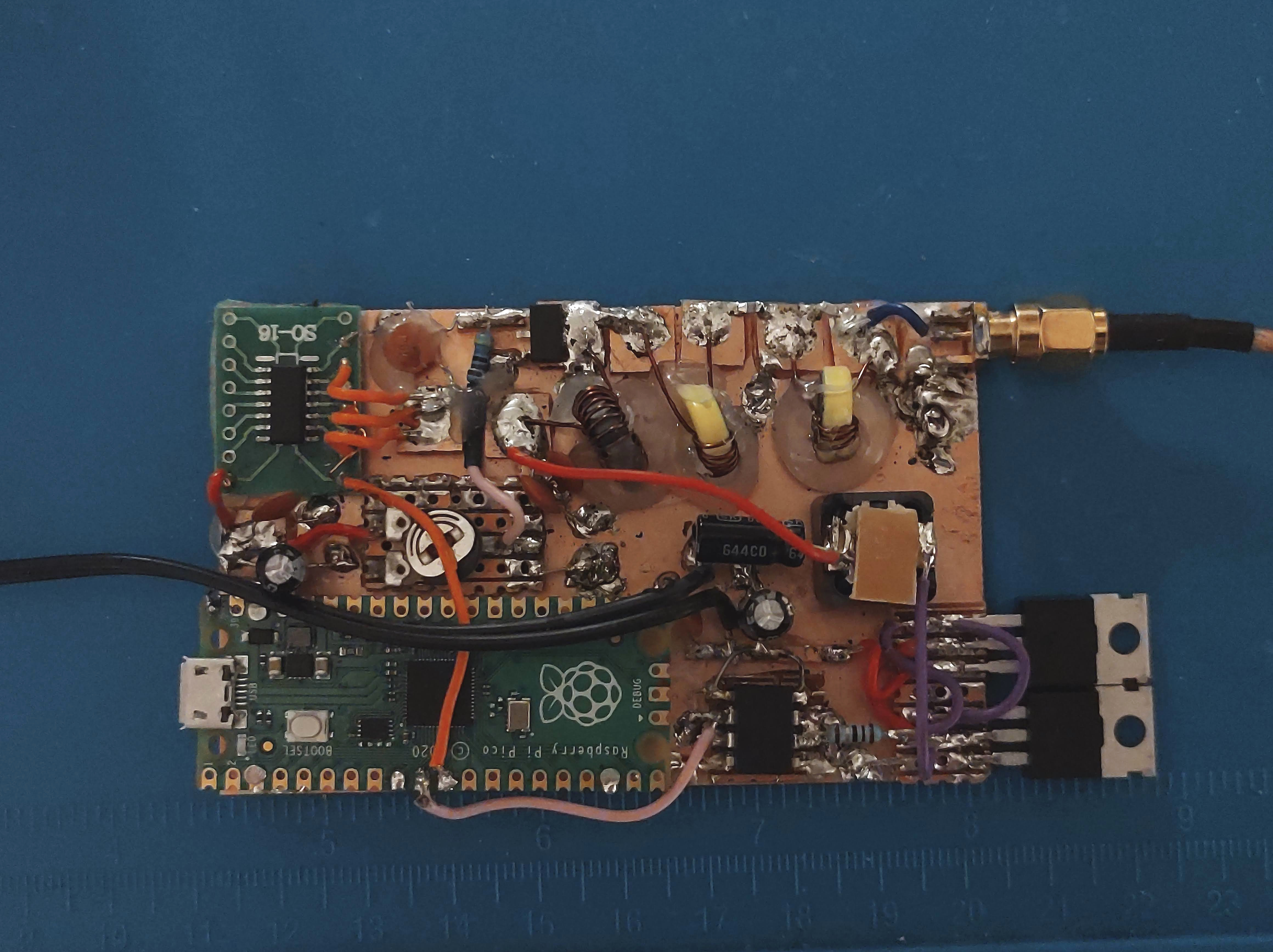
A prototype of the class-E amplifier was built using copper-clad board. For this experiment, the 20M band was chosen using a centre frequency of 14.175MHz. The analogue switch that we previously used to mix the envelope with the RF output is no longer needed. The polar modulated amplifier is in effect a high-power unbalanced mixer.
Note:
The software now has a compile time option to output balanced or unbalanced PWM outputs. The original design used a balanced mixer, but the polar-modulated amplifier requires an unbalanced output.
//nco.cpp
#ifdef BALANCED //Use with FDT5351 balanced mixer
pwm_set_gpio_level(m_magnitude_pin, 128 + (magnitude >> 9));
pwm_set_gpio_level(m_magnitude_pin + 1, 128 - (magnitude >> 9));
#else //Use with polar modulated amplifier
//remove 8 lsbs
magnitude >>= 8;
pwm_set_gpio_level(m_magnitude_pin, magnitude);
pwm_set_gpio_level(m_magnitude_pin + 1, 255 - magnitude);
#endif
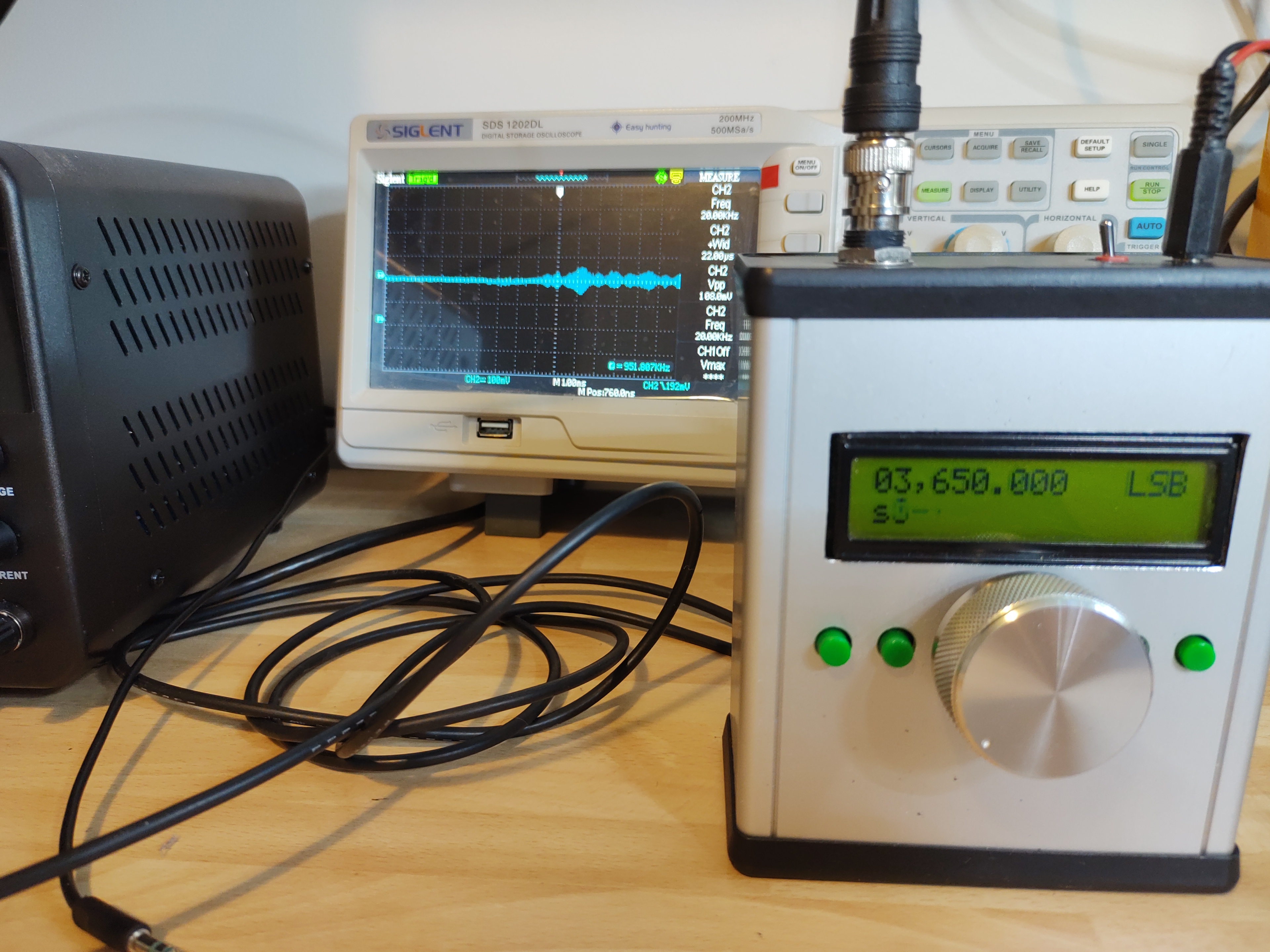
The prototype used a combination of through-hole and surface mount components, whatever I had lying around. In the class-E amplifier, it is important to use NP0/C0G type capacitors rated for 100V or more. The L3 winding forms part of the second harmonic notch filter, the frequency of the notch can be measured using a nanoVNA, and fine adjustments can be made to the notch frequency by adjusting the spacing of the inductor windings. With the calculated number of turns the frequency was too low, to achieve the correct frequency at twice the fundamental it was necessary to remove a whole turn.
The amplifier was then connected and further adjustments were made. It was also necessary to remove a turn from L1 to achieve the desired power output level. Further tweaks to the bias voltage and the turn spacing on L2 to achieve the best efficiency. I found it difficult to measure the efficiency with sufficient accuracy to give a confident efficiency figure. In practical terms, however, it was possible to achieve an output power of close to 5 watts into a dummy load. Although the transistor did get a little warm, it didn’t overheat and the case temperature leveled off at around 44 degrees C.
Class-D Audio Amplifier
Now that the class-E amplifier is providing amplification of the RF signal, retaining the frequency and phase information it is necessary to modulate the amplitude. The amplifier modulating the amplitude also needs to provide high efficiency, so it makes sense to use a switching amplifier here too. The design implements a very simple class-D audio amplifier. The basis of the design is a MOSFET half bridge using a p-channel and n-channel MOSFET. Although there are probably plenty of devices that could be used n this amplifier I have chosen the IRF510 and IRF9510. There are devices with much better RDS-on specifications, but these devices are fairly ubiquitous, and can easily handle the switching frequency.
Although it is possible to use n-channel MOSFETS for the high side of the bridge, this would complicate the gate driving arrangement. This simpler arrangement allows both halves of the bridge to be driven with a single gate driver. Initially, I had concerns that this might lead to shoot-through, a condition where both transistors a momentarily switched on simultaneously. I had planned to work around this issue by using complementary PWM outputs with their switching times sufficiently spaced. In practice, this didn’t seem to be necessary. The output of the amplifier is passed through a second-order LC low-pass filter. I used a PWM frequency of nearly 500kHz, I tried to increase this value as far as possible to reduce ripple. This could be further reduced by using a higher order filter, although the choke feeding the class-E amplifier should also help to block ripple.
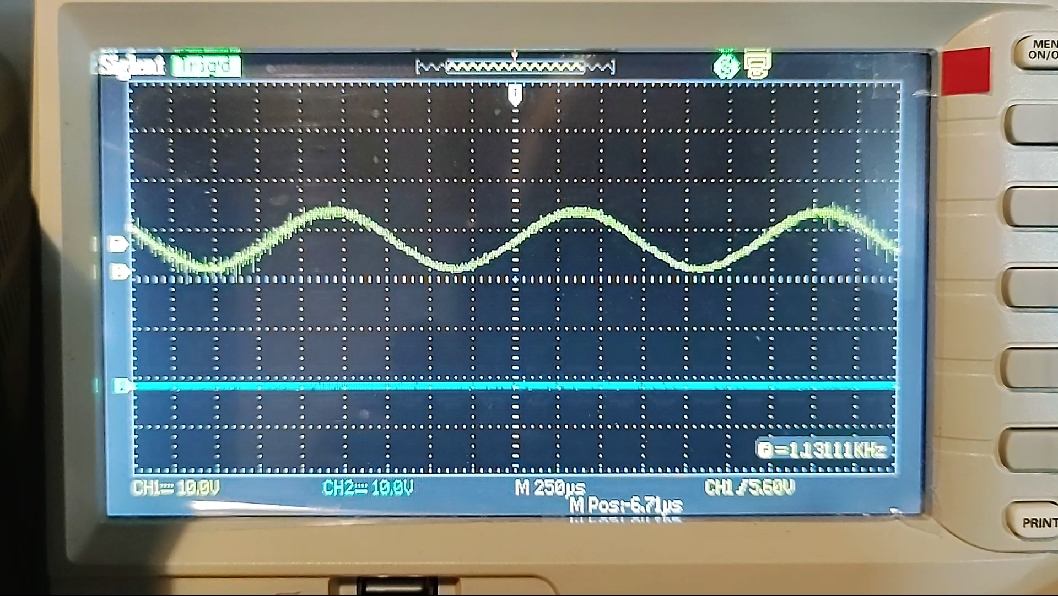
After passing through the low-pass filter, the PWM waveform now resembled a sinusoid. This sinusoid represents the RF envelope (a single-tone AM modulated) that provides the power supply to the class-E amplifier.
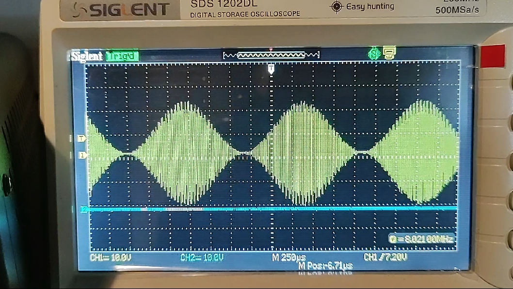
The RF output from the class-E amplifier now contains an amplitude-modulated RF signal.
Testing
I tested the amplifier in single-sideband mode, comparing the output to the previous unamplified audio. Subjectively speaking the quality of the audio was very similar to the unamplified audio and no noticeable distortion had been introduced. Check out the Video to see the results.
Spurious Emissions
The output of the amplifier was connected (via an attenuator) to a tinySA to analyze the frequency spectrum of the signal. The resonant filters in the Class-E amplifier have effectively filtered out the second and third harmonics, reducing them to acceptable levels. However, some spurious emissions, a couple of MHz from the fundamental frequency, are present. While these spurious signals are 30dB below the fundamental, their relatively low power level, only a few milliwatts, still has the potential to cause interference on other frequencies. Unfortunately, the output quality is insufficient for practical use on the air.
I conducted brief investigations and determined that the spurious signals are caused by the periodic frequency corrections. Choosing a transmit period that is an exact division of the clock frequency eliminates these spurious emissions. The frequency corrections create spurs in the frequency spectrum due to their repeated periodic pattern.
To mitigate these spurious emissions, a common method is to apply phase dithering. By adding a statistically random pattern to the corrections, they manifest as noise spread across the spectrum rather than as spikes. However, implementing phase dithering in this design is challenging because the waveforms are pre-generated. While randomizing transitions in prerecorded waveforms is possible, they remain the same each time they are replayed. Dynamically updating the waveforms might not be practical on a Pi Pico.
Another potential solution is additional filtering. Unfortunately, the spurs are close to the fundamental frequency, requiring a very high-quality filter, which could be challenging and expensive to implement.
The most effective solution may be to prevent the need for frequency corrections altogether. Utilizing a Phase-Locked Loop (PLL) could be the best approach, as many QRP transmitter designs employ PLLs such as the SI5351. These I2C programmable devices offer good frequency resolution and minimal jitter. Several methods could be considered. A PLL could be used as the clock for the Pi Pico, if the pico is clocked at a multiple of the transmit frequency, this would avoid the need for frequency adjustments. Another solution would be to modulate the phase by sending frequency adjustments to the PLL via I2C, similar to the approach used by the uSDX design. Alternatively, we could employ the more traditional method of using a Quadrature Phase Exciter, converting an IQ signal into a phase and amplitude modulated RF signal using analog circuitry.
Transmitter Examples
transmitter_microphone_example.cpp
This is a very minimal usage example, the transmit mode and frequency are hard coded. Audio input is taken from a microphone using the builtin ADC.
transmitter_serial_example.cpp
This is a more complete usage example, the transmit mode and frequency are controlled through the USB serial interface. Audio data is streamed from a host PC via the USB serial connection.
The example may be controlled using the transmit.py utility.
The original transmitter used an FST3253 analog switch as a balanced mixer. In this design, two PWM outputs provide complimentary “balanced” inputs to the mixer. One non inverted output swings between 0 and VCC/2, the inverted output swings between vcc/2 and vcc.
The polar modulated amplifier behaves as an unbalanced mixer. It only requires a single PWM output that swings between 0 and vcc. However the second (inverted) pwm output has been retained as this allows ether inverting or non-inverting gate drivers to be used.
To allow both hardware variants to be used, two build targets have been defined for each of the transmitter examples.
transmitter_microphone_example_mixer.uf2 and transmitter_serial_example_mixer.uf2 support the FST3253 mixer design.
transmitter_microphone_example_polar_amplifier.uf2 and transmitter_serial_example_polar_amplifier.uf2 support the polar amplifier design.
A simple transmitter application is included in transmitter_serial_example.cpp. This allows the frequency and mode to be selected, and also to allow transmit data to be streamed through the USB Serial Interface.
The transmitter expects audio data in 8-bit signed format. The expected sample rate depends on the transmit mode.
Mode |
Sample Rate kS/s |
|---|---|
FM |
15 |
AM |
12.5 |
LSB |
10 |
USB |
10 |
The sox utility can be used to convert from most common audio formats.
#generate a file to send in SSB mode
sox FileToConvert.mp3 -t s8 -r 10k myfile.wav
Using the Python Transmit Utility
A simple python utility can stream audio files over USB to the transmitter.
To send audio using FM modulation at 10MHz.
$python transmit.py test_file_15k.wav
Available Ports
0 /dev/ttyS4: n/a [n/a]
1 /dev/ttyACM0: Pico - Board CDC [USB VID:PID=2E8A:000A SER=E6609CB2D37B9828 LOCATION=1-1:1.0]
Select COM port >
1
Enter Frequency Hz>
10000000
Enter mode AM/FM/LSB/USB >
FM
To send audio using USB modulation at 14.175MHz.
$python transmit.py test_file_10k.wav
Available Ports
0 /dev/ttyS4: n/a [n/a]
1 /dev/ttyACM0: Pico - Board CDC [USB VID:PID=2E8A:000A SER=E6609CB2D37B9828 LOCATION=1-1:1.0]
Select COM port >
1
Enter Frequency Hz>
14.175e6
Enter mode AM/FM/LSB/USB >
USB
If you would like to support 101Things, buy me a coffee: https://ko-fi.com/101things